Wednesday, 30 December 2015
VLSI DESIGN SPECIFICATION
VLSI DESIGN:
--->Very Large Scale Integration (VLSI) describes about semiconductor integrated circuits which composed of hundreds of thousands of memory cells logic elements. It is the technique of implementation circuit designing that provides computational speed.
CARRY LOOK AHEAD ADDER
--->In ripple carry adders, the carry propagation time is the major speed limiting factor.
--->Most other arithmetic operations, e.g. multiplication and division are implemented using
several add/subtract steps. Thus, improving the speed of addition will improve the speed
of all other arithmetic operations.
--->The addition of two binary numbers in parallel implies that all the bits of augend and addend available for computation at the same time.
--->Pi=Ai^Bi;
--->Gi=Ai&Bi;
--->The output sum and carry can be expressed as
--->Si=Pi^ci;
--->Ci+1=Gi+PiCi;
HOW TO AVOID PARALLEL CASE STATEMENT?
Example is the same as Example 4 except that a Synopsys "parallel_case" directive has been added to the case header. This example will simulate like a priority encoder but will infer nonpriority encoder logic when synthesized.
module intctl1b (int2, int1, int0, irq);
output int2, int1, int0;
input [2:0] irq;
reg int2, int1, int0;
always @(irq) begin
{int2, int1, int0} = 3'b0;
casez (irq) // synopsys parallel_case
3'b1??: int2 = 1'b1;
3'b?1?: int1 = 1'b1;
3'b??1: int0 = 1'b1;
endcase
end
endmodule
VEDIC MULTIPLIER
--->We know general decimal multiplication.
--->We use Binary multiplication.
--->Here i am going to explain Vedic multiplication.
--->Multiplication is one of the main functions in a Digital Signal Processing System. The overall performance of the DSP system depends on the performance of the multiplier.
--->Hence it is very important to develop an efficient and fast design to implement multiplier. Vedic mathematics can be used to transform tedious calculations into simpler and orally manageable operation.
--->Vedic multiplication uses Urdhva Triyambakam multiplication algorithm.
--->The Vedic multiplication algorithm generates partial products in parallel. In this work, we propose using Han-Carlson adder to improve the performance of Vedic multiplier.
What is a "parallel" case statement?
Example shows a casez statement
that is not parallel because if the 3-bit irq bus is 3'b011,
3'b101, 3'b110 or 3'b111, more
than one case item could potentially match the irq value. This
will simulate like a priority
encoder where irq[2] has priority over irq[1], which has priority over
irq[0]. This example will also infer a priority
encoder when synthesized.output int2, int1, int0;
input [2:0] irq;
reg int2, int1, int0;
always @(irq) begin
{int2, int1, int0} = 3'b0;
casez (irq)
3'b1??: int2 = 1'b1;
3'b?1?: int1 = 1'b1;
3'b??1: int0 = 1'b1;
endcase
end
endmodule
FOR MORE DETAILS CLICK HERE
HOW TO AVOID NON-"FULL" CASE STATEMENTS?
It shows a case statement for a 3-to-1 multiplexer that is not "full" but the case header
includes a "full_case" directive. During Verilog simulation, when binary pattern 2'b11 is driven onto the select lines, the y-output will behave as if it were latched, the same as in Example but the synthesis will treat the y-output as a "don't care" for the same select-line combination, causing a functional mismatch to occur between simulation and synthesis
module mux3b (y, a, b, c, sel);
output y;
input [1:0] sel;
input a, b, c;
reg y;
always @(a or b or c or sel)
case (sel) // synopsys full_case
2'b00: y = a;
2'b01: y = b;
2'b10: y = c;
endcase
endmodule
NON-"FULL" CASE STATEMENTS
It shows a case
statement for a 3-to-1 multiplexer that is not "full." The case
statement
does not define
what happens to the y-output when binary pattern 2'b11 is driven onto the
select lines. In this example, the Verilog simulation will hold the last
assigned y-output value and synthesis will infer a latch on the y-output as
shown in the latch inference
module mux3a (y, a, b, c, sel);
output y;
input [1:0] sel;
input a, b, c;
reg y;
always @(a or b or c or sel)
case (sel)
2'b00: y = a;
2'b01: y = b;
2'b10: y = c;
endcase
endmodule
Friday, 18 December 2015
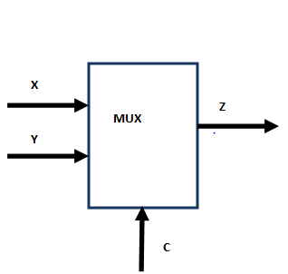
VERILOG MULTIPLEXER
MULTIPLEXER:
Module mux2_1(out,control,in1,in2);
input control,in1,in2;
output out;
assign out=control?in1:in2;
endmodule
--->Conditional expression?true expression:false expression
--->If the control is evaluated it is assigned to 1,then in1 is assigned to out, else in2.
FOR MORE REFERENCE CLICK HERE
Module mux2_1(out,control,in1,in2);
input control,in1,in2;
output out;
assign out=control?in1:in2;
endmodule
--->Conditional expression?true expression:false expression
--->If the control is evaluated it is assigned to 1,then in1 is assigned to out, else in2.
FOR MORE REFERENCE CLICK HERE
Monday, 14 December 2015
CMOS TAPERED BUFFER DESIGN
--->The buffer consists of a chain of inverter stages where width of
each MOS transistor in a stage is increased by a constant factor
(called taper factor) than that of the transistors in the previous stage.
--->The model is named as split capacitor model as output
capacitance and input capacitance of each stage is modeled
separately.
--->The constant increase in width of transistors in each
stage provides fixed ratio of output current drive to output
capacitance and hence equal rise, fall, and delay times for each
stage. Here Ci denotes the input capacitance of minimum size
inverter, Cd
denotes the drain capacitance of minimum size
inverter, Cload denotes the load capacitance of the last stage
inverter, N denotes number of stages in the buffer chain and F
denotes the scaling factor per stage in the inverter buffer chain.
Sunday, 13 December 2015
BUFFER DESIGN USING CMOS TECHNOLOGY
BUFFER DESIGN:

Power dissipation and propagation delay in CMOS buffers driving large capacitive loads and proposes a CMOS buffer design for improving power dissipation at optimized propagation delay. The reduction in power dissipation is achieved by minimizing short circuit power and subthreshold leakage power which is predominant when supply voltage (VDD) and threshold voltage (Vth) are scaled for low voltage applications in deep sub micron (DSM) region.
Large capacitive loads are often present in CMOS integrated circuits and tapered buffers are used to drive these large capacitive loads at high speed, while ensuring that the load placed on previous stages of the signal path is not too large.These buffers are used in the memory access path as word-line drivers, to drive large off-chip capacitances in I/O circuits, and in clock trees to ensure that skew constraints are satisfied. But,deployment of these buffers in high-performance systems imposes a power overhead on each instance regardless to its actual performance.High-performance VLSI design is attracting much attention because of emerging need for miniaturization, and hence design optimization for trading-off power and performance in nano meter scale integrated circuits is the need of the present scenario, which demands a decrease in both supply voltage VDD(to maintain low power dissipation) and threshold voltage Vth (to sustain propagation delay reduction), but the fact is that the decrease in Vth not only increases leakage power but also short circuit power. while working in nano scale technology the total power dissipation of clock.

Saturday, 12 December 2015
ENERGY-EFFICIENT APPROXIMATE MULTIPLICATION FOR DIGITAL SIGNAL PROCESSING
Embedded and mobile computing devices are frequently required to execute some key digital signal processing (DSP) and classification applications. To further improve energy efficiency of executing such applications, first, dedicated specialized processors are often integrated in computing devices. It has been reported that the use of such specialized processors can improve energy efficiency by 10–100× compared with general-purpose processors at the same voltage and technology generation. Second, many DSP and classification applications heavily rely on complex probabilistic mathematical models and are designed to process information that typically contains noise. Thus, for some computational error, they exhibit graceful degradation in overall DSP quality and classification accuracy instead of a catastrophic failure. Such computational error tolerance has been exploited by trading accuracy with energy consumption.
In order to motivate and describe our proposed multiplier, we define an m-bit segment as m contiguous bits starting with the leading one in an n-bit positive operand. We dub this method dynamic segment method (DSM) in contrast to static segment method (SSM) that will be discussed later in this section. With two m-bit segments from two n-bit operands, we can perform a multiplication using an m × m multiplier. Fig. 1 shows an example of a multiplication after taking 8-b segments from 16-b operands. In this example, we can achieve 99.4% accuracy for a 16 × 16 multiplication even with an 8 × 8 multiplier.
Subscribe to:
Comments (Atom)


