Monday, 25 April 2016

VLSI circuit design for low power

VLSI circuit design for low power:
The growing market of portable (e.g., cellular phones, gaming consoles, etc.), battery-powered electronic systems demands microelectronic circuits design with ultra low power dissipation. As the integration, size, and complexity of the chips continue to increase, the difficulty in providing adequate cooling might either add significant cost or limit the functionality of the computing systems which make use of those integrated circuits. As the technology node scales down to 65nm there is not much increase in dynamic power dissipation. However the static or leakage power is same as or exceeds the dynamic power beyond 65nm technology node.
Hence the techniques to reduce power dissipation is not limited to dynamic power. In this article we discuss circuit and logic design approaches to minimize Dynamic, Leakage and Short Circuit power dissipation. Power optimization in a processor can be achieved at various abstract levels . System/Algorithm/Architecture have a large potential for power saving even these techniques tend to saturate as we integrate more functionality on an IC. So optimization at Circuit and Technology level is also very important for miniaturization of ICs.
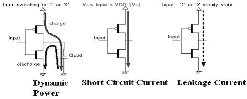
Total Power dissipated in a CMOS circuit is sum total of dynamic power,short circuit power and static or leakage power. Design for low-power implies the ability to reduce all three components of power consumption in CMOS circuits during the development of a low power electronic product. In the sections to follow we summerize the most widely used circuit techniques to reduce each of these components of power in a standard CMOS design.


leakage current in fet


Dynamic Power Suppression
Dynamic/Switching power is due to charging and discharging of load capacitors driven by the circuit. Supply voltage scaling has been the most adopted approach to power optimization, since it normally yields considerable power savings due to the quadratic dependence of switching/dynamic power PSwitching on supply voltage VDD. However lowering the supply voltage affects circuit speed which is the major short-coming of this approach. So both design and technological solutions must be applied to compensate the decrease in circuit performance introduced by reduced voltage. Some of the techniques often used to reduce dynamic power are described below.

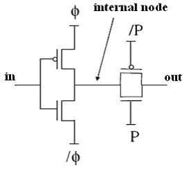
Adiabatic Circuits
In adiabatic circuits instead of dissipating the power is reused. By externally controlling the length and shape of signal transitions energy spent to flip a bit can be reduced to very small values. Since diodes are thermodynamically irreversible they are not used in the design of Adiabatic Logic. MOSFETs should not be turned ON when there is significant potential difference between source and drain. And should not be turnoff when there is a significant current flowing through the device.
FOR MORE DETAIL CLICK HERE


Recent Trends In VLSI Design Applications


Digital System Design:

                             The digital system design is nothing but the embedded systems, which forms a part or many parts in a simple or complex system. The program can be a high level like C or C++ or any hardware language (HDL) like VHDL/or Verilog. However, the complexity of high level language restrains the use by many of designers; rather they prefer to use HDL languages. Hence, it is felt that the use of VHDL helps in the verification process in various stages to ensure the correctness of the stages before entering to the next.


A model of a digital circuit is an abstract by a modeling language. Such a language is preferred here to VHDL/ Verilog. However, the object oriented language like C++ has an extension to it, called System C, to be one such language, which could be used for this purpose too.

 Software Augmentation:  
                              Although many authors has spelt out various design methods, however, the recent methodology is the process of augmentation of the application software into the hardware (application circuit/device) itself. The application software developed for any application devices is programmed & stored in a memory (slave Device) though the FPGA (target device) on any Software Plat form like Xilinx. The FPGA has been embedded into a Spartan6 Xilinx Platform. The memory could be an on board SRAM, or any external SRAM, and the display device could be a LCD/or SSD/or LEDs. This could be done as described below: The very initial step is to perform the study of requirements and done the analysis for both hardware and software essentialities & constraints. Then the hardware & software constraints are resolved. Once the constrains are removed, the hardware design is performed, in a concurrent mode. Then the software is made ready. The paper discussed here, has been chosen for the FPGA on Spartan6 Xilinx platform. The HDL used here is VHDL. The application software is programmed suitably. Last but not the least, is the augmentation of software into the application devices. Our co-authors have already selected various sensors for their applications. Accordingly, the program has been verified through the built in ISim software tools for the proper timing and correctness of the design. This paper is a collective effort of our engineers for their projects, in realization of Modeling, Simulation & Implementation of various communication protocols in our projects using VHDL language and using appropriate hard -wares as required & at KCTRONICS Innovative Services Private Limited, Bangalore.


Language (VHDL): 
The language, VHDL has been divided into two constructs such as Entity (ii) architecture. The entity is a pre defined word and the architecture is a relationship between input & outputs of the systems bound to the entity. This binding helps in the visibility of the entity to the architecture. The system can be designed with the use of VHDL language on the Xilinx platform, FPGA being as the target device where the application program can be stored for the purpose of application devices.


Monday, 4 January 2016

BLOCKING AND NON BLOCKING ASSIGNMENTS

BLOCKING ASSIGNMENTS:
--->The assignment must complete before the line is executed.
--->Operator is = use in blocking assignment.

NON BLOCKING ASSIGNMENTS:
--->The right hand side is evaluated immediately.
---->Operator is<=
always @(posedge clk)
 begin 
word[15:8] <= word[ 7:0]; 
word[ 7:0] <= word[15:8];
 end


FOR MORE REFERENCE CLICK HERE

Wednesday, 30 December 2015

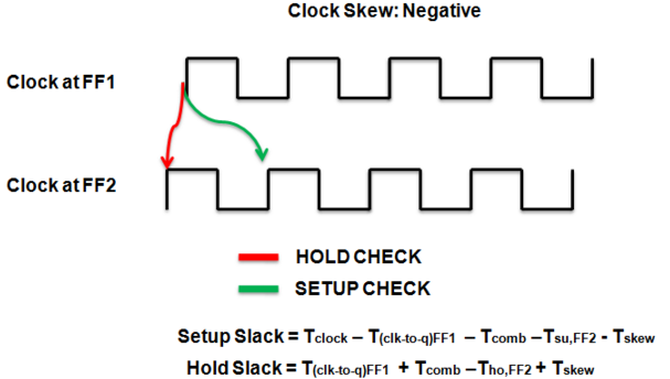
CLOCK SKEW

CLOCK:
--->The variations in a local clock edge relative to a master clock reference.
--->The difference between arrival times of the clock at different devices is called skew.


FOR MORE REFERENCE CLICK HERE

VLSI DESIGN SPECIFICATION

VLSI DESIGN:
--->Very Large Scale Integration (VLSI) describes about semiconductor integrated circuits which composed of hundreds of thousands of memory cells logic elements. It is the technique of implementation circuit designing that provides computational speed.

CARRY LOOK AHEAD ADDER

--->In ripple carry adders, the carry propagation time is the major speed limiting factor.
--->Most other arithmetic operations, e.g. multiplication and division are implemented using several add/subtract steps. Thus, improving the speed of addition will improve the speed of all other arithmetic operations.
--->The addition of two binary numbers in parallel implies that all the bits of augend and addend available for computation at the same time.

--->Pi=Ai^Bi;
--->Gi=Ai&Bi;
--->The output sum and carry can be expressed as
--->Si=Pi^ci;
--->Ci+1=Gi+PiCi;


HOW TO AVOID PARALLEL CASE STATEMENT?


         Example  is the same as Example 4 except that a Synopsys "parallel_case" directive has been added to the case header. This example will simulate like a priority encoder but will infer nonpriority encoder logic when synthesized.

module intctl1b (int2, int1, int0, irq);
output int2, int1, int0;
input [2:0] irq;
reg int2, int1, int0;
always @(irq) begin
{int2, int1, int0} = 3'b0;
casez (irq) // synopsys parallel_case
3'b1??: int2 = 1'b1;
3'b?1?: int1 = 1'b1;
3'b??1: int0 = 1'b1;
endcase
end
endmodule